- Product Innovation & Lifecycle
- Advanced Engineering

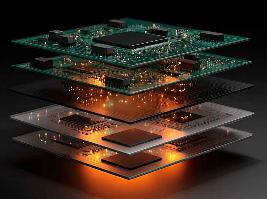
VVDN transforms complex electrical schematics into reliable, high-performance physical hardware platforms. Whether your design requires ultra-compact form-factor routing, ultra-high-speed digital interfaces (like DDR5 or PCIe Gen 5/6) or complex multi-domain RF isolation, our engineering ecosystem delivers production-ready PCB layouts. We adapt completely to your workflow, functioning either as an agile, standalone routing partner or as a seamless extension of your internal R&D organization.
By inherently coupling our layout process with strict Design for Manufacturability (DFM) and Design for Testability (DFT) rules while running concurrent pre- and post-layout simulations, we eliminate costly structural board re-spins and drastically slash your time-to-market.
The true differentiator of our service is The Fabrication Advantage. VVDN owns advanced, in-house electronics manufacturing facilities and our PCB designers work under a continuous feedback loop with our actual factory assembly lines. Every trace width, via stack-up and panelization choice is pre-optimized for high automated manufacturing yields from day one.
From schematic capture to production-ready layouts, VVDN delivers precision PCB design for complex electronic systems.


We conform entirely to your company's native software ecosystem to ensure absolute cross-compatibility and clean file handoffs.
Get production-ready manufacturing packages—including Gerber X2, ODB++, and IPC-2581 data sets—fully cleared of DFM constraints and pre-optimized for automated assembly lines.
Our PCB layout engineers sit directly beside our in-house Signal Integrity (SI) and thermal simulation specialists to check and correct trace issues in real-time.
Early access to hardware design guidelines from major chip vendors ensures your complex processor breakouts match exact reference standards.
Reduce development cycles through concurrent design, simulation, DFM validation and manufacturing collaboration, minimizing costly redesigns and board re-spins.

Send over your layout constraints, mechanical DXF outlines or schematic sheets for a completely secure, non-disclosure-backed engineering analysis.

 Global


