Overview

VVDN Technologies, with its world-class manufacturing facilities provide clients full turnkey solutions for their products and production needs. The fully automated high speed PCB assembly lines are capable of assembling complex boards with components including BGAs, uBGA’s, PLCC, FPGA, Bare dies, flip chips, OSC,3D Coplan etc. With scrutinized systems for batch production and component traceability, our PCB assembly process ensures the best quality of finished products to customers across the globe.
VVDN PCB ASSEMBLY facility

  • World-class SMT lines
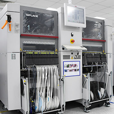
  • Package-on-Package(PoP), Special component chip mounting, and fine pitch high count BGA capability
  • Supports maximum PCB size of upto 850 mm x 560 mm
  • Precision Placement – 01005 metric to 200x125x25 SMT to Chip On Board
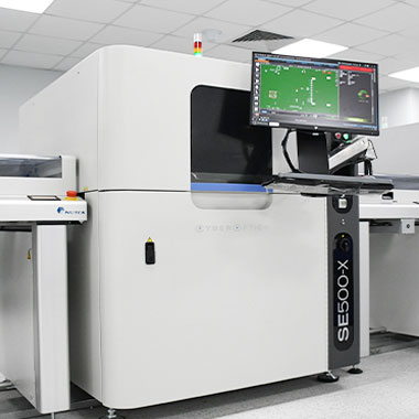
  • Robust inspection: In-line 3D AOI and 3D SPI
  • High-Speed multi mounters rated total CPH 693500, selective, robotic and wave soldering machine for non-SMD parts
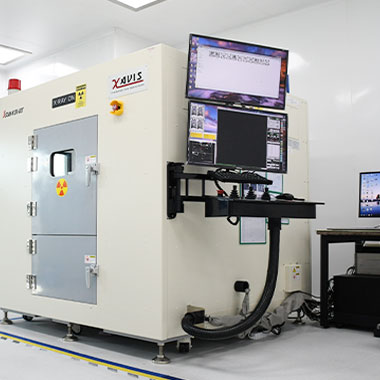
  • 2D and 3D X-Ray Machine (AXI)
  • End-to-end traceability
  • Functional test, in-circuit test (ICT), and burn in test (BIT)

insight stories

See how we helped enterprises across the globe to change and transform the world by bringing the new to life with the latest technologies

Interested In VIRTUAL TOUR OF VVDN's MANUFACTURING FACILITIES?
Stay updated with
our latest offerings