


Continuously evolving Wi-Fi Technologies, rising customer expectations, and increasing use cases of Wi-Fi from unlicensed radio links to crowded IoT devices, have put extra pressure on the device supporting components. Amongst all, RF is the one that always comes first in the picture. While the CPU acts as the brain of the device, RF functions as the ears, whose performance defines the performance of the device.
We began with 802.11a and have now moved to the 802.11ax standard. This increases the complexity of RF manifolds and demands a high level of engineering expertise to provide an optimized solution. RF design is a step-by-step process that consists of RF circuit design, component selection, Antenna design, and Testing/Validation. Each step is equally important to maximize the performance of the device. While one blog will not be sufficient to explain all the building blocks, we will touch upon the critical factors of RF circuits in this blog.
Table of Contents
RF Circuit
In terms of designing a solution, RF circuit design is the initial and the most important step. The RF circuit includes circuit design, component selection, and convenient debugging in case any issues pop up. RF circuit is a vast subject that requires a lot of R&D and knowledge to design a Wi-Fi solution. Hardware design engineers always need to keep a few important basics in mind while designing a Wi-Fi solution.
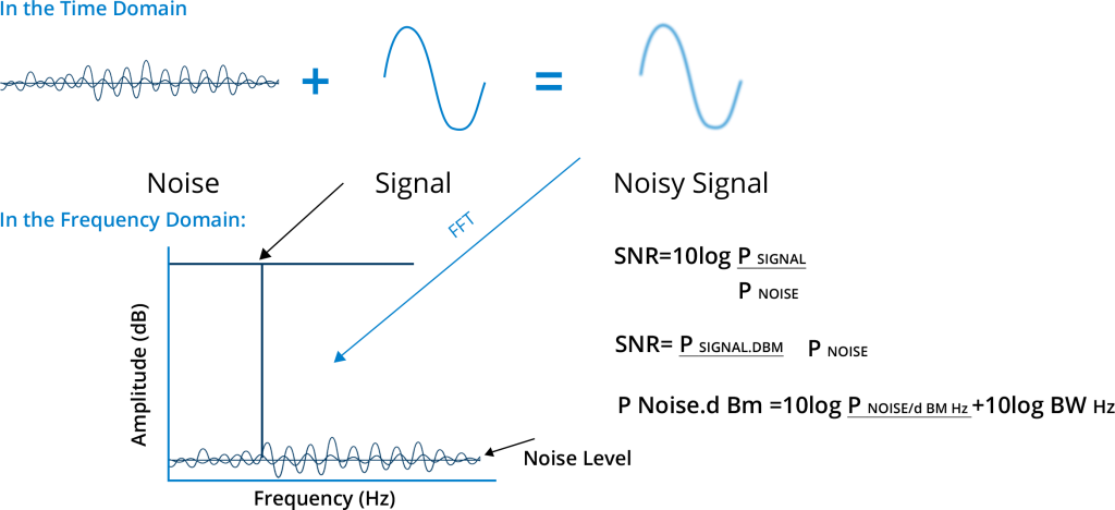
- Signal to Noise Ratio (SNR): One of the most critical factors is the Signal to Noise ratio (SNR) which identifies how much the signal is affected by the noise. The level of noise is inversely proportional to the quality of the signal. At times, noise integrates with the signal so well that even a noisy signal looks fine at an oscilloscope. However, when it is converted to frequency, it clearly shows the signal and the noise level separately. The logarithmic ratio between them is signal to noise ratio and more gaps will lead to better signal.
- Noise Factor: Noise figure (NF) and noise factor (F) are measures of degradation of the signal-to-noise ratio (SNR), which are caused by components in a signal chain. The noise factor of a component is the ratio of input SNR to output SNR. However, The complete RF circuit design consists of multiple stages and every further component introduced induces some noise and the next LNA/PA amplifies it, as shown in the figure.
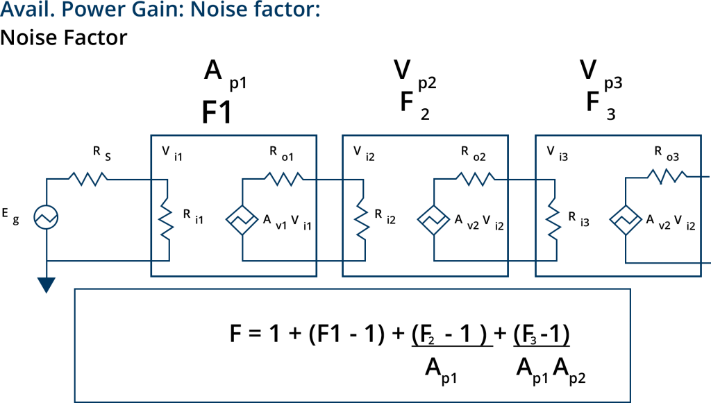
It becomes highly important for RF engineers to choose the first element that will have minimum Noise contribution or low noise factor which is going to create the difference between a good or a bad circuit.
- Noise Figure: Noise Figure (10log F >= 0dB, where F is noise factor) is when we compare the designed circuit with an ideal circuit with zero noise. In other words, the noise figure is simply the noise factor expressed in decibels (dB). It defines the health of our RF circuit. Noise figures can never be negative which means that the output can never be better than input. The whole idea is to have the minimum NF value or as close to zero as possible while designing an RF circuit.
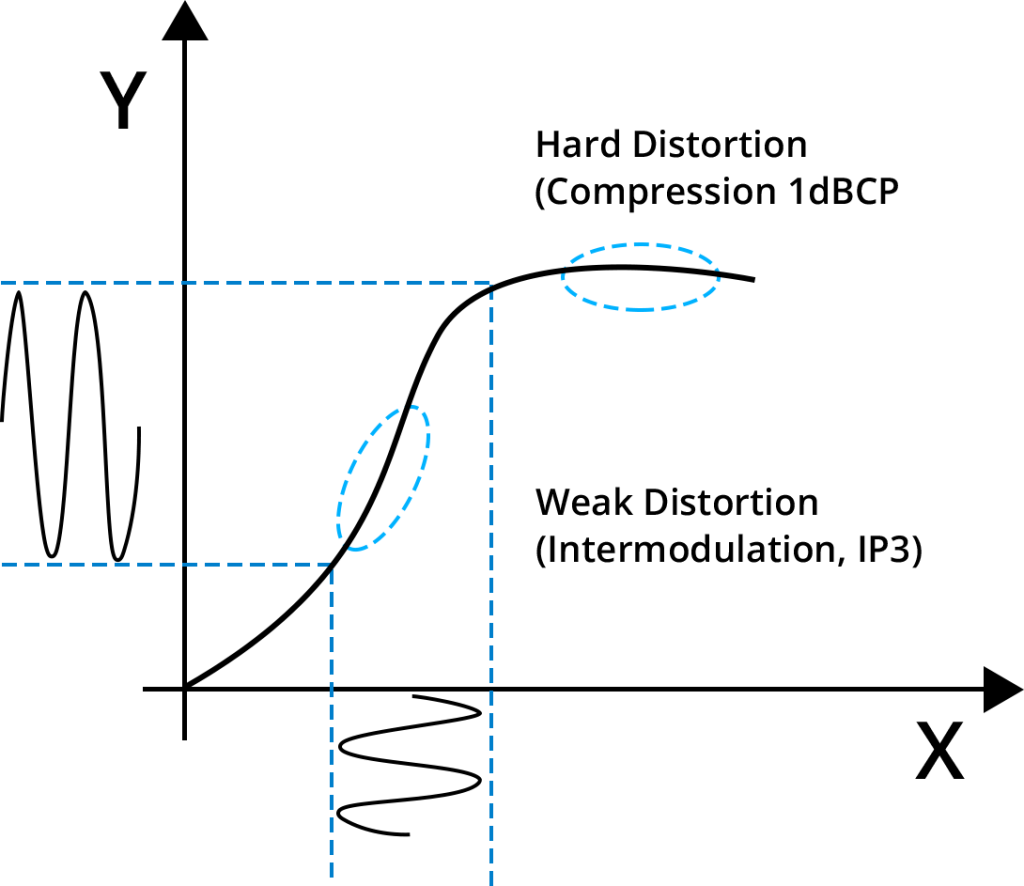
- Distortion: Moreover, the Tx should send a good signal which is audible to Rx. With the Tx, comes a very common problem, distortion, which means the loss of original shape and gain of the signal. This generally happens because of the non-linear characteristics of the FEM module. This distortion can be divided into two types – Hard Distortion and Weak Distortion. Hard Distortion (signal clamping) distorts the upper amplitude of the signal and changes the original shape of the signal. Weak Distortion (generation of harmonics) adds overtones that are whole number multiples of an original wave’s frequencies. Both of these distortions cause 3 major things – gain compression, blocking & desensitization, and intermodulation (IP2, IP3).
- Phase noise: This generally occurs from crystal oscillators, so an engineer should choose a good quality oscillator to avoid this issue.
- Image reflection: Image reflection comes up during the mixing of signals at RFIC on the Rx side, which can cause serious issues in the circuit and can go undetected many times. This can be taken care of by rejecting the image reflection and adding a 90-degree shift image to the original.
- Filters: To filter the received signal, the Surface Acoustic Wave (SAW)/Bulk Acoustic Wave (BAW) is used to receive only the desired bands. These have “Q” of hundreds but are not tunable. So to remove the interference, which is a grave concern, SAW filters play an important role and remove the out-of-band frequencies. To remove the in-band frequencies, in-band blockers are used after the down-conversion.
- Other Consideration: Apart from this, an RF Engineer must consider impedance matching, antenna specifications, losses because of circuits, switches(TDD), a duplexer(FDD), etc to arrive at exact calculations. If we talk about the Rx end, every antenna possesses some sensitivity level, indicating the minimum level of signal it can detect with given SNR. It provides a reference for reverse engineering for selecting components and arrangements. All the main architectures for Rx are touched in the below sections.
Architectures
While we have gone through some of the major considerations above, there are few architectures like Super Heterodyne, Low IF, Direct Conversion, Direct Sampling, RF Sampling, etc. in practice that has out-of-band pros and cons. We will cover a high-level overview of the architectures used in the Wi-fi domain.
- Super Heterodyne is the legacy architecture that generally offers great sensitivity and is easy to process at low frequencies. Moreover, it is a two-stage architecture as shown in the diagram below. Here, IR filter (image rejection), Lo1, IF filter (intermediate frequency) provide the best possible filtering of the signal, and LO2 helps in regenerating the signal into baseband signal for processing.
The disadvantage with Super Heterodyne is the number of components required which makes it a costly solution. This results in a higher chance of spurs because of the local oscillators and nonlinear components in the circuit.

- Direct Sampling is the most widely used architecture these days, especially for Wi-Fi circuits. On average, 70-80% of Wi-Fi circuits are built using Direct Sampling architecture. Its low power consumption and lesser space requirements in the IF chain and better image frequency rejection make it a popular choice. In this architecture, the signals go through filters followed by Analog IQ Demodulator which mixes the signal with 90 degrees shifted signal generated from LO. This helps remove the image signal, however, some DC components evade the baseband signals which can later be removed by the Complex Analog baseband filters.

Although, the problem with this architecture is the self-mixing of the LO signal through the mixer because of the signal leakage through capacitors, etc. This mixing generates a DC signal and after amplification, it becomes a major problem for the processor. So to remove this issue, a simple capacitor can be used to block the DC components after the mixing stage and high-level shields to isolate the RF circuits from each other. In the case of a few designs required in the upcoming 5G technologies, automatic gain calibration is used which we would be explaining in another blog.
- RF Sampling architecture is a relatively new concept where signal mixing and filtering are done in the digital domain. This is the opposite of Direct Sampling where we do the same steps in the analog domain. Here, the components required are much lesser but the cost is much higher compared to that in Direct Sampling. This architecture is most likely to be more popular in the years to come where we would need many high-frequency architectures.
Link Budget Analysis
Apart from the above, the link budget calculations tell us, how far the signal can be transmitted and what will be the throughput? Several factors may impact the performance of a radio system in the real deployment scenarios like, available and permitted output power, antenna gains, available bandwidth, receiver sensitivity, radio technology, and environmental conditions. A simple formula to calculate the signal strength is:
Received Power (dBm) = Transmitted Power (dBm) + Gains (dB) − Losses (dB)
If the estimated received power is sufficiently high as compared to the Rx sensitivity (Link Margin), the link budget is considered sufficient for transmitting data. The major losses that occur in the real deployment scenarios are as follows:
- Free-Space Path loss: Loss of signal strength due to environmental factors such as humidity, temperature, etc.
- Multipath loss: When waves travel along different paths which leads to unwanted interference and out-of-phase signals at Rx end to cancel each other.
- Cabling loss: Refers to the amount of Power Loss over a Cable’s Length.
- RF Connector loss: Losses that occur due to connector material or loose connectors
How Does VVDN Help OEMs/NEMs?
VVDN leverages its vast expertise in the field of RF (Radiofrequency) engineering. The RF engineering team at VVDN has extensive years of experience in the domain and specializes in transmission systems, PCB design, and layout, RF tuning & calibration, RF circuit evaluation, embedded design, customization & placement of antennas in the devices for optimum performance. VVDN has capabilities for custom design antennas, RF circuit design, and validation. VVDN follows all communication and regulatory standards for RF such as IEEE and 3GPP for safety as well as ensuring radio waves are not interfering with each other. VVDN has successfully developed and manufactured products ranging from low-powered trackers, smartwatches to outdoor access points and radio units in the field of 5G where RF plays a significant role. RF tuning, calibration, and pre-certification product testing are all done at VVDN’s dedicated in-house RF testing labs which are equipped with the latest equipment.